F12N
PowerPC MPC5200B CPU Board

Hauptmerkmale
- 32-bit/33-MHz cPCI system slot, 4 HP
- MPC5200B / 384 MHz
- FPGA 18,752 LEs (approx. 225,000 gates)
- Up to 256 MB onboard DDR SDRAM
- Up to 8 MB boot Flash, NAND Flash
- 2 MB SRAM, 16 MB graphics memory
- Dual Fast Ethernet, COM, USB (front)
- Dual CAN bus controller
- FPGA for user-defined I/O functions
- MENMON BIOS for PowerPC cards
- -40°C to +85°C with qualified components
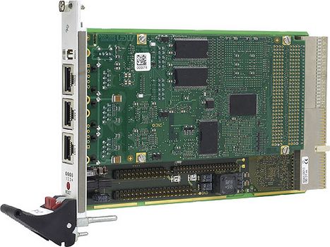
Equipped with the MPC5200B PowerPC, the F12N single-board computer is a versatile 3U Eurocard CompactPCI board that operates at up to 400 MHz and 700 MIPS. The F12N is designed especially for systems which require low power consumption and mechanical robustness. With the processor consuming less than 1 W, the board is delivered for -40 to +85°C operation temperature. All components on the board are soldered. The F12N is thus well placed as a rugged computing platform for mobile applications, offering thewhole world of Linux based software and real-time operating support for VxWorks and QNX.
The CPU card is equipped with an onboard soldered SDRAM of up to 256 MB and up to 1 GB NAND Flash as well as with 16 MB additional SDRAM, up to 8 MB boot Flash and 2 MB battery-backed SRAM.
The SBC provides two Fast Ethernet interfaces, one serial line and USB 1.1 at its front panel. As an alternative to RJ45, D-Sub connectors guarantee reliable functions also in harsh environments. Two CAN controllers with V2.0A/BCAN protocol are included in the MPC5200B and are accessible via SA-Adapters. A second serial interface can be accessed using an SA-Adapter on the F12N. (E)IDE and GPIO are also on board.
The large FPGA on the F12N allows to realize additional user-defined functions such as graphics, touch, further serial interfaces, further CAN bus controllers, binary I/O etc. for the needs of the individual application in a very flexible way. Before boot-up of the system, the FPGA is loaded from boot Flash. Updates ofthe FPGA contents can be made inside the boot Flash during operation. The FPGA functions can be physically implemented by using SA-Adapters. A maximum of 8 SA-Adapters can be used on the F12N and I/O can be made accessible at the front panel.
Equipped with a PCI-bridge chip, the F12N offers a full CompactPCI interface (system slot functionality) for reliable system expansion.
The F12N comes with MENMON support. This firmware/BIOS can be used for bootstrapping operating systems (from disk, Flash or network), for hardware testing, or for debugging applications without running any operating system.
- MPC5200B
- Up to 400MHz
- 2x16KB L1 data and instruction cache integrated in MPC5200
- Up to 256MB SDRAM system memory
- Soldered
- DDR
- 64MHz memory bus frequency
- Up to 1GB soldered NAND Flash (and more), FPGA-controlled
- 16MB additional SDRAM, FPGA-controlled, e.g. for video data and NAND Flash firmware
- Up to 8MB boot Flash
- 2MB GoldCap-backed SRAM, or: 128KB non-volatile FRAM
- Serial EEPROM 8kbits for factory settings
- Parallel IDE (PATA)
- One IDE port via 44-pin onboard connector
- FPGA-controlled
- PIO mode 0 support
- Up to 1GB soldered ATA NAND Flash (and more), FPGA-controlled
- USB
- One USB 1.1 port
- Type A connector at front panel
- OHCI implementation
- Data rates up to 12Mbit/s
- Ethernet
- Two 10/100Base-T Ethernet channels
- One channel FPGA-controlled
- Two RJ45 or one D-Sub connector at front panel
- One RS232 UART (COM1)
- RJ45 or D-Sub connector at front panel
- Data rates up to 115.2kbit/s
- 512-byte transmit/receive buffer
- Handshake lines: CTS, RTS
- One UART (COM10)
- Accessible via I/O connector
- Physical interface at front panel using SA-Adapter via 10-pin ribbon cable on I/O connector
- RS232..RS485, isolated or not: for free use in system (e. g. cable to front)
- Data rates up to 115.2kbit/s
- 16-byte transmit/receive buffer
- Handshake lines: CTS, RTS; DCD, DSR, DTR; RI
- CAN bus
- Two CAN bus channels
- 2.0 A/B CAN protocol
- Data rates up to 1 Mbit/s
- Connection via onboard connectors
- External transceivers using SA-Adapters
- GPIO
- 36 GPIO lines
- FPGA-controlled
- Connection via onboard I/O connector
- Further I/O depending on FPGA configuration
- One USB 1.1 (Type A)
- Two Ethernet (RJ45)
- One RS232 UART (RJ45)
- Standard factory FPGA configuration:
- Main bus interface
- 16Z070_IDEDISK - IDE controller for NAND Flash
- 16Z043_SDRAM - Additional SDRAM controller (16MB)
- 16Z023_IDENHS - IDE controller (PIO mode 0; non-hot-swap)
- 16Z087_ETH - Ethernet controller (10/100Base-T)
- 16Z025_UART - UART controller (controls COM10)
- 16Z034_GPIO - GPIO controller (40 lines, 5 IP cores)
- The FPGA offers the possibility to add customized I/O functionality. See FPGA.
- Real-time clock with GoldCap backup
- Power supervision and watchdog
- Reset button, GPIO-controlled
- Three user LEDs, GPIO-controlled; 1 FPGA power status LED
- Compliance with CompactPCI Core Specification PICMG 2.0 R3.0
- System slot
- 32-bit/32-MHz PCI-to-PCI bridge
- V(I/O): +3.3V or +5V (Universal Board)
- Supply voltage/power consumption, CompactPCI standard version:
- +5V (-3%/+5%), 10mA max.
- +3.3V (-3%/+5%), 1A typ.
- Supply voltage/power consumption, stand-alone version:
- +5V (-3%/+5%), 800mA typ.
- Uses 5V only
- MTBF: 277,234h @ 40°C according to IEC/TR 62380 (RDF 2000)
- Dimensions: conforming to CompactPCI specification for 3U boards
- Weight: 250g
- Temperature range (operation):
- -40..+85°C
- Airflow: min. 10m³/h
- Temperature range (storage): -40..+85°C
- Relative humidity (operation): max. 95% non-condensing
- Relative humidity (storage): max. 95% non-condensing
- Altitude: -300m to + 3,000m
- Shock: 15g/11ms
- Bump: 10g/16ms
- Vibration (sinusoidal): 2g/10..150Hz
- VxWorks
- Linux (ELinOS)
- QNX
- MSCAN/Layer2 support: Modular Driver Interface System (MDIS for all supported operating systems)
- For more information on supported operating system versions and drivers see Software.